


dsPIC Memory Organization
The dsPIC microcontroller's memory is divided into Program Memory and Data Memory. Program Memory (ROM) is used for permanent saving program being executed, while Data Memory (RAM) is used for temporarily storing and keeping intermediate results and variables.
Program Memory (ROM)
Program Memory (ROM) is used for permanent saving program code being executed, and it is divided into several sections, as on the picture below. The size of these sections is device dependant.
The program memory map is divided into the User Memory Space and Configuration Memory Space. The User Memory Space contains the Reset vector, interrupt vector tables, program memory and data EEPROM memory (dsPIC30 family and some PIC24 family MCU's).
The Configuration Memory Space contains non-volatile configuration bits for setting device options and the device ID locations.
Program Memory (ROM) Organization
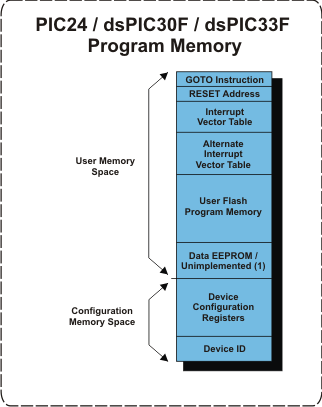
Legend :
- dsPIC33F Program Memory Organization
Data Memory (RAM)
Data memory consists of :
- SFR Memory Space
- X and Y Data RAM
- DMA RAM (only for dsPIC33F Family)
- Unimplemented Memory Space
Data Memory (RAM) Organization
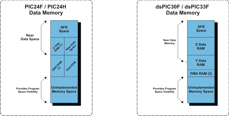
Legend :
- PIC24F Data Memory Organization
- dsPIC33F Data Memory Organization
SFR Memory Space
The first 2kB of data memory is allocated to the Special Function Registers (SFRs). The SFRs are control and status register for core and peripheral functions in the dsPIC.
X and Y Data RAM
Up to 8 kB of data RAM is implemented after the SFRs. This is general purpose RAM that can be used for data storage. This RAM is split into X and Y memory for dsPIC instructions.
This allows DSP instructions to support dual operand reads, so that data can be fetched from X and Y memory space at the same time for a single instruction.
The X and Y data space boundary is fixed for any given device. When not doing DSP instructions, the memory is all treated as a single block of X memory.
DMA RAM
Every dsPIC33F device contains a portion of dual ported DMA RAM located at the end of Y data space. Direct Memory Access (DMA) is a very efficient mechanism of copying data between peripheral SFRs and buffers or variables stored in RAM, with minimal CPU intervention.
The DMA controller can automatically copy entire blocks of data without requiring the user software to read or write the peripheral Special Function Registers (SFRs) every time a peripheral interrupt occurs.
The DMA controller uses a dedicated bus for data transfers and therefore, does not steal cycles from the code execution flow of the CPU. To exploit the DMA capability, the corresponding user buffers or variables must be located in DMA RAM.
Unimplemented Memory Space
The last segment of data RAM space is not implemented, but can be mapped into program space for Program Space Visibility. This allows program memory to be read as though it were in data RAM.
 Notes :
- Boundaries between memory spaces are device specific. Please, refer to the appropriate datasheet for details.
- Memory spaces are not shown to scale. Please, refer to the appropriate datasheet for details.
There are seven memory type specifiers that can be used to refer to the data memory: rx, data, code, sfr, xdata, ydata, and dma
Program Space Visibility Address Generation
The upper 32 Kbytes of the data memory address space may be optionally mapped into program memory space pages. This mode of operation is called Program Space Visibility (PSV).
When PSV is enabled, the compiler will generate Program Space Visibility Addresss differently than the physical (effective) address. This is so-called "compiler (PSV) address".
The 15 LSbs of the physical address are provided by the working register that contains the physical address; the MSb of the working register (bit 15) is not used to form the address.
Instead, the MSb specifies whether to perform a PSV access from program space (MSb = 1) or a normal access from data memory space (MSb = 0).
If a working register effective address of 0x8000 or greater is used, the data access will occur from program memory space when PSV is enabled. All accesses will occur from data memory when the working register physical address is less than 0x8000.
The remaining address bits are provided by the physical address, as shown in picture :
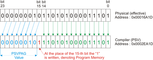
The physical address bits are concatenated with the 15 LSbs of the working register to form a 23-bit Program Space Visibility Address.
What do you think about this topic ? Send us feedback!
Find them on
